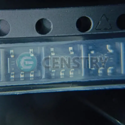
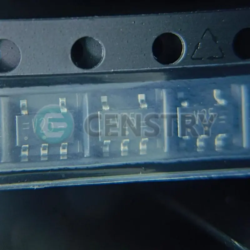
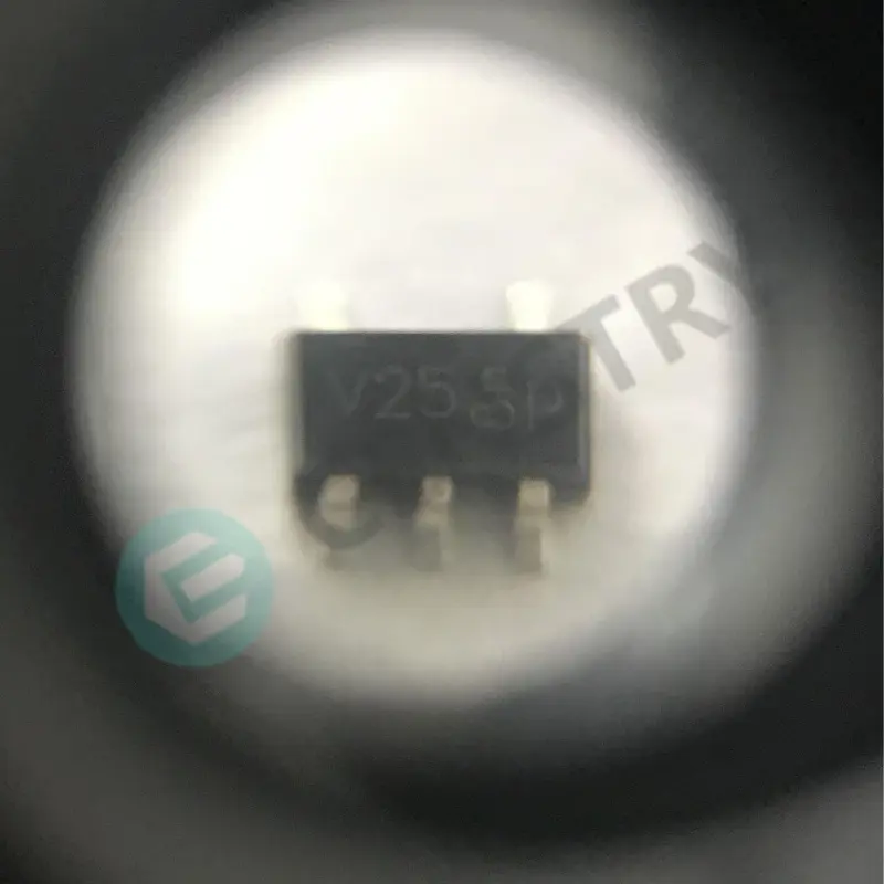
IC BUFFER NON-INVERT 5.5V SC74A


Le immagini servono solo come riferimento.
Consulta le specifiche del prodotto per i dettagli del prodotto.
IC BUFFER NON-INVERT 5.5V SC74A
Gli ordini superiori a $ 200 hanno diritto a un regalo in stile cinese in edizione limitata.
Gli ordini superiori a $ 1000 beneficiano di un'esenzione dalle spese di spedizione di $ 30.
Gli ordini superiori a $ 5000 beneficiano dell'esenzione dalle spese di spedizione e di transazione.
Queste offerte sono applicabili sia ai clienti nuovi che a quelli esistenti e sono valide dal 1 gennaio 2024 al 31 dicembre 2024.
NXP
74LVC1G125GV datasheet
SOT753
Chip IC
 Lead free/RoHS Compliant
Invia la tua richiesta di preventivo adesso e prevediamo di fornirti un preventivo entro maggio 03, 2024. Effettua ora il tuo ordine e prevediamo di completare la transazione entro maggio 07, 2024. Ps: L'orario è secondo GMT+8:00.


FEATURES
• Wide supply voltage range from 1.65 V to 5.5 V
• High noise immunity
• Complies with JEDEC standard:
– JESD8-7 (1.65 V to 1.95 V)
– JESD8-5 (2.3 V to 2.7 V)
– JESD8B/JESD36 (2.7 V to 3.6 V).
• ±24 mA output drive (VCC = 3.0 V)
• CMOS low power consumption
• Latch-up performance exceeds 250 mA
• Direct interface with TTL levels
• Inputs accept voltages up to 5 V
• Multiple package options
• ESD protection:
– HBM EIA/JESD22-A114-B exceeds 2000 V
– MM EIA/JESD22-A115-A exceeds 200 V.
• Specified from −40 °C to +85 °C and −40 °C to +125 °C.
DESCRIPTION
The 74LVC1G125 is a high-performance, low-power,
low-voltage, Si-gate CMOS device, superior to most
advanced CMOS compatible TTL families.
The input can be driven from either 3.3 V or 5 V devices.
This feature allows the use of this device in a mixed
3.3 V and 5 V environment.
This device is fully specified for partial power-down
applications using Ioff. The Ioff circuitry disables the output,
preventing the damaging backflow current through the
device when it is powered down.
The 74LVC1G125 provides one non-inverting buffer/line
driver with 3-state output. The 3-state output is controlled
by the output enable input (OE). A HIGH level at pin OE
causes the output to assume a high-impedance
OFF-state.


Request a quote 74LVC1G125GV at censtry.com. All items are new and original with 365 days warranty! The excellent quality
and guaranteed services of 74LVC1G125GV in stock for sale, check stock quantity and pricing,
view product specifications, and order contact us:sales@censtry.com.
The price and lead time for 74LVC1G125GV depending on the quantity required, please send your request to us,
our sales team will provide you price and delivery within 24 hours, we sincerely look forward to cooperating with you.
Silicon
5958 PCS
SM662GXC-ACS .PDF
Silicon
6779 PCS
SM662PXC-BD .PDF
Silicon
4503 PCS
SM662GXC-BD .PDF
GigaDevice
6588 PCS
GD25S512MDYIGR .PDF
2024-05-02
Excellent supplier- George and Andy are true closers - Thanks for the business!
2024-05-02
Fast and reliable company
2024-05-02
Fast service, fair price and good product, thank you.
2024-05-01
Gabi is easy to deal with. Parts came in on time. Will deal with again. Gretchen
2024-05-01
Good and reliable company
2024-04-30
Quick and Easy
2024-04-29
Good company, excellent sales
2024-04-26
Good cooperation
2024-04-21
Good part , all good .
2024-04-10
Good service and good parts
Apprezziamo molto il tuo feedback. Per favore condividi la tua recensione più genuina.
*Effettua l'accesso al tuo account prima di pubblicare un commento