agosto 25, 2023
1512
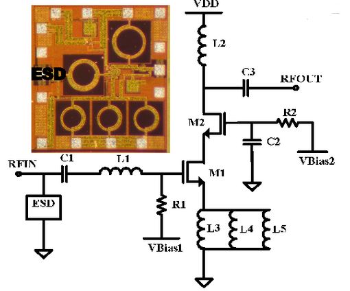
In recent years, with the rapid development of wireless communication technology, Radio Frequency Integrated Circuits (RFICs) have gained widespread attention as a crucial component within wireless communication systems. Among them, Complementary Metal-Oxide-Semiconductor (CMOS) RFIC design stands as a pivotal force, playing a vital role in achieving high-performance, low-power wireless communication systems.
In the past, due to limitations in CMOS fabrication processes, RF circuits often utilized specialized technologies such as BiCMOS and SiGe. However, as CMOS technology advanced and process sizes decreased, CMOS RFICs began to showcase unique advantages such as cost-effectiveness, high integration, and strong reliability.

Radio Frequency Integrated Circuit (RFIC) design is a specialized process focusing on circuit design within the Radio Frequency (RF) frequency range. This RF range typically spans from several megahertz (MHz) to several gigahertz (GHz) and is employed in various applications like wireless communication, radar, satellite communication, and wireless sensor networks.
The goal of RFIC design is to implement various functions within specific frequency ranges, such as signal amplification, frequency mixing, modulation/demodulation, filtering, and power amplification. Relative to digital or low-frequency analog circuits, RF circuit design faces greater challenges due to complexities arising from high-frequency characteristics, noise, and signal distortion.
Frequency Characteristics: RF circuit behavior can vary at different frequencies, necessitating maintenance of the desired frequency response during design.
Impedance Matching: Impedance matching is critical to ensure maximal signal transfer between circuits. In RF design, this is crucial as impedance mismatches could lead to signal reflection and energy loss.
Noise: Noise is a pronounced issue in RF circuits. Designers must consider noise reduction strategies to preserve system sensitivity.
Nonlinearity: Many devices exhibit nonlinear characteristics at high frequencies, potentially causing signal distortion. Designers need to account for these nonlinear effects.
Power Consumption: Power consumption of high-frequency circuits, particularly in applications like mobile devices, is a significant consideration.
Electromagnetic Compatibility (EMC): EMC becomes more sensitive in high-frequency environments, necessitating considerations to prevent unnecessary inter-circuit interference.

Despite the opportunities brought by CMOS technology development for RFIC design, it has also introduced a series of challenges. Among them, the following points are crucial considerations in design:
1.High-Frequency Loss: CMOS materials experience significant losses at high frequencies, impacting signal transmission quality. Designers need suitable techniques to mitigate losses, such as optimizing transmission line structures and selecting appropriate packaging materials.
2.Device Nonlinearity: RF signals often have significant amplitudes, and CMOS devices exhibit nonlinear effects under large signal conditions, leading to increased distortion. Thus, designers need techniques like distortion and circuit structure optimization to suppress nonlinear effects.
3.Device Parameter Variation: The CMOS process introduces device parameter variations, demanding performance stability for RF circuits. Designers can employ adaptive calibration and temperature compensation techniques to address parameter variation impacts.
To tackle the aforementioned challenges, designers have proposed innovative techniques to optimize CMOS RFIC performance:
| Technique | Features and Applications |
| Broadband Matching | Applied to circuits with a wide signal frequency range, Applied to circuits with a wide signal frequency range. |
| Low-Noise Amplifier Design | Enhances sensitivity in receiver systems,suitable for demanding signal reception. |
| Efficient Power Amplifier Design | Improves transmitter system energy efficiency, enhancing signal transmission range. |
| Adaptive Calibration | Compensates for device parameter variations, enhancing circuit performance stability. |
| Temperature Compensation | Counteracts performance fluctuations caused by temperature changes through calibration. |

CMOS RFIC design finds widespread applications in various fields. From 5G communication to the Internet of Things (IoT), radar systems to satellite communication, high-performance RFICs are integral. Looking ahead, as technology advances, CMOS RFIC design will encounter more opportunities and challenges. Innovations in architecture, higher integration, and complex system integration are likely.
The following are the current practical applications and prospects of CMOS radio frequency integrated circuits:
| Application Area | Current Applications | Outlook |
|---|---|---|
| 5G Communication | Achieving high-speed, stable wireless communication transmission. | Increasing demand for higher frequencies and broader bandwidths driving RF innovation. |
| Internet of Things (IoT) | Providing low-power, long-range communication for IoT devices. | Increasing demand for miniaturization and multi-module communication. |
| Radar Systems | Enabling target detection, tracking, and more. | Enhanced precision and multifunctionality in radar systems. |
| Satellite Communication | Providing reliable communication links between satellites and ground stations. | Larger capacity and more stable satellite communication networks. |
With ongoing technological progress, the application of emerging technologies in CMOS RF design has become a research focus. The following are applications of emerging technologies in CMOS RF design:
| Technology | Features and Applications |
|---|---|
| Smart Antenna Array Technology | Combines RF circuit design and signal processing for signal directionality and beamforming, enhancing communication coverage and signal quality. Suitable for improving wireless network performance and reducing interference. |
| Mixed-Signal Design with Digital-Assisted Calibration | Integrates digital-assisted calibration techniques into RF analog circuits for real-time performance calibration. Helps counteract process variations, and temperature effects, and maintain optimal circuit performance. |
| Machine Learning-Based Optimization | Utilizes machine learning algorithms to optimize RF circuit design. Accelerates the design process, identifies optimal design parameters, and may lead to more efficient and innovative designs. |
| Exploration of Nanotechnology | Incorporates nano-materials and devices to enhance RF circuit performance. Potential benefits include improved frequency response, reduced power consumption, and noise, enabling higher performance in compact designs. |
Mod-01 Lec-01 RF system basic architectures
CMOS RFIC design plays a pivotal role in wireless communication, with its performance crucial to overall communication system effectiveness. Continuous innovation and technological advancements are expected to bring forth remarkable breakthroughs in CMOS RFIC design. From low-noise amplifiers to smart antenna arrays, from broadband matching to digital-assisted calibration, the fusion and innovation of various technologies will propel RFIC design to new heights. With ongoing progress in fabrication processes, CMOS RFIC design will encounter more opportunities and challenges, shining even brighter in the future.